1. Introduction to SMD Packaging Technology
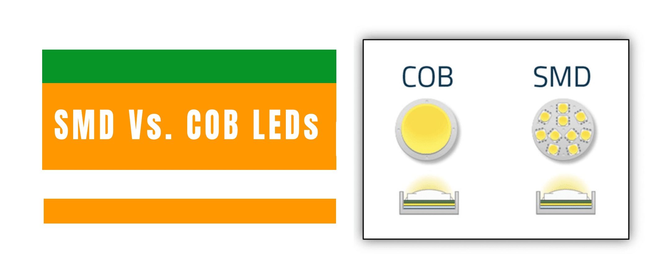
1.1 Definition and Background of SMD
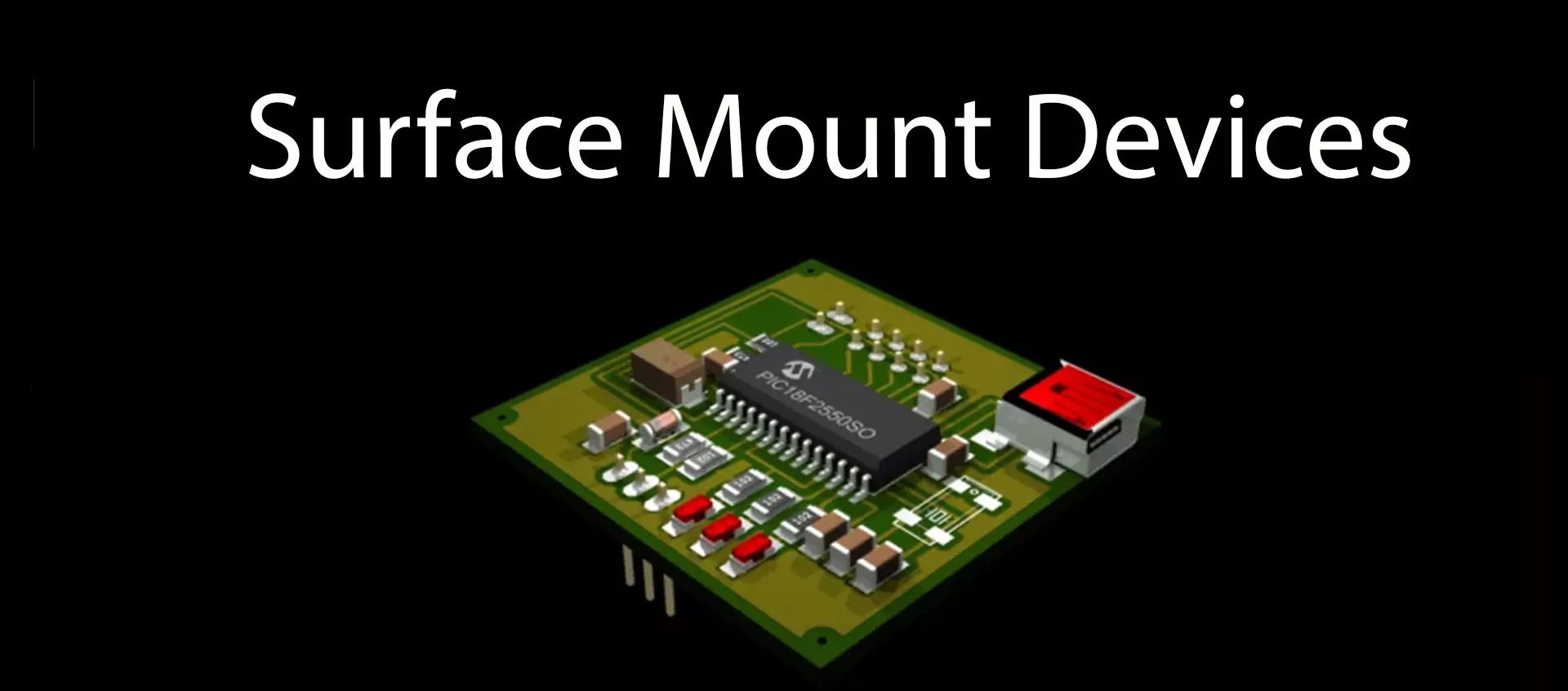
SMD packaging technology is a form of electronic component packaging. SMD, which stands for Surface Mounted Device, is a technology widely used in the electronics manufacturing industry for packaging integrated circuit chips or other electronic components to be directly mounted on the surface of the PCB (Printed Circuit Board).
1.2 Main Features
Small Size: SMD packaged components are compact, enabling high-density integration, which is beneficial for designing miniaturized and lightweight electronic products.
Light Weight: SMD components do not require leads, making the overall structure lightweight and suitable for applications that require reduced weight.
Excellent High-Frequency Characteristics: The short leads and connections in SMD components help reduce inductance and resistance, enhancing high-frequency performance.
Suitable for Automated Production: SMD components are suitable for automated placement machines, increasing production efficiency and quality stability.
Good Thermal Performance: SMD components are in direct contact with the PCB surface, which aids in heat dissipation and improves thermal performance.
Easy to Repair and Maintain: The surface-mount method of SMD components makes it easier to repair and replace components.
Packaging Types: SMD packaging includes various types such as SOIC, QFN, BGA, and LGA, each with specific advantages and applicable scenarios.
Technological Development: Since its introduction, SMD packaging technology has become one of the mainstream packaging technologies in the electronics manufacturing industry. With technological advancements and market demand, SMD technology continues to evolve to meet the needs for higher performance, smaller sizes, and lower costs.
2. Analysis of COB Packaging Technology
2.1 Definition and Background of COB
COB packaging technology, which stands for Chip on Board, is a packaging technique where chips are directly mounted on the PCB (Printed Circuit Board). This technology is primarily used to address LED heat dissipation issues and achieve tight integration between the chip and the circuit board.
2.2 Technical Principle
COB packaging involves attaching bare chips to an interconnect substrate using conductive or non-conductive adhesives, followed by wire bonding to establish electrical connections. During packaging, if the bare chip is exposed to air, it can be contaminated or damaged. Therefore, adhesives are often used to encapsulate the chip and bonding wires, forming a “soft encapsulation.”
2.3 Technical Features
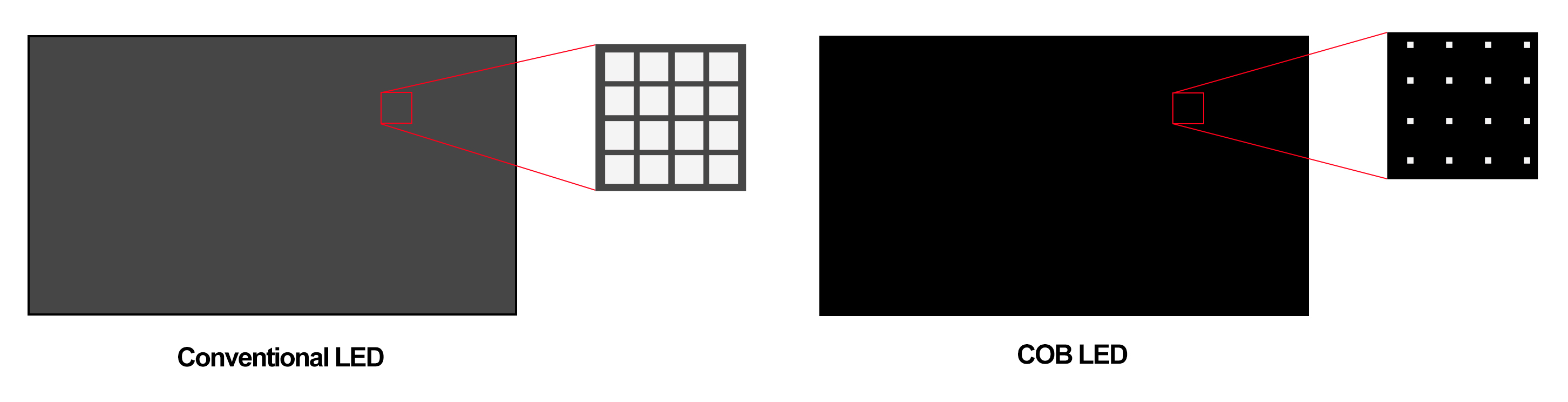
Compact Packaging: By integrating packaging with the PCB, chip size can be significantly reduced, integration level increased, circuit design optimized, circuit complexity lowered, and system stability improved.
Good Stability: Direct chip soldering on the PCB results in good vibration and shock resistance, maintaining stability in harsh environments such as high temperature and humidity, thereby extending product lifespan.
Excellent Thermal Conductivity: Using thermal conductive adhesives between the chip and PCB effectively enhances heat dissipation, reducing thermal impact on the chip and improving chip lifespan.
Low Manufacturing Cost: Without the need for leads, it eliminates some complex processes involving connectors and leads, reducing manufacturing costs. Additionally, it allows for automated production, lowering labor costs and improving manufacturing efficiency.
2.4 Precautions
Difficult to Repair: Direct soldering of the chip to the PCB makes individual chip removal or replacement impossible, typically requiring the replacement of the entire PCB, increasing costs and repair difficulty.
Reliability Issues: Chips embedded in adhesives can be damaged during the removal process, potentially causing pad damage and affecting production quality.
High Environmental Requirements: The COB packaging process demands a dust-free, static-free environment; otherwise, the failure rate increases.
3. Comparison of SMD and COB
So, what are the differences between these two technologies?
3.1 Comparison of Visual Experience
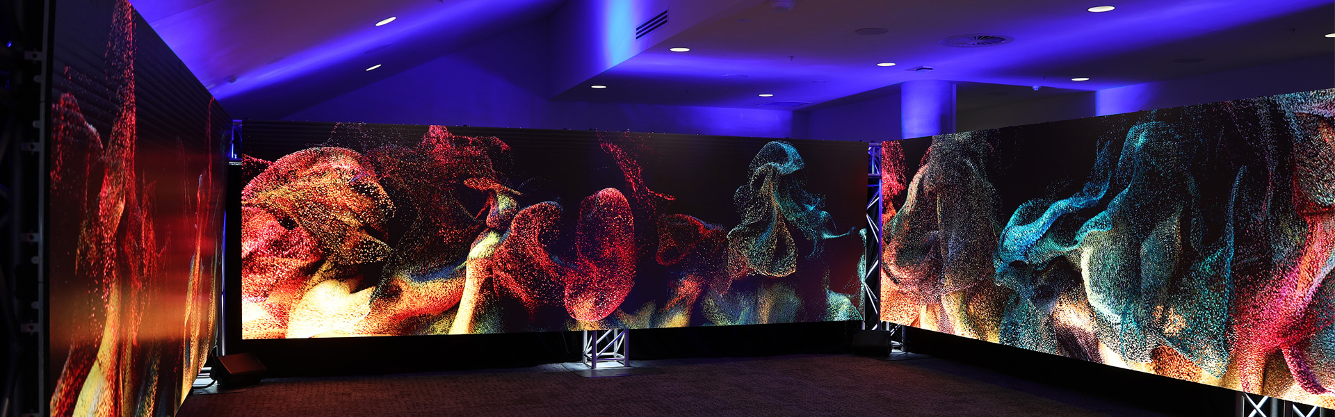
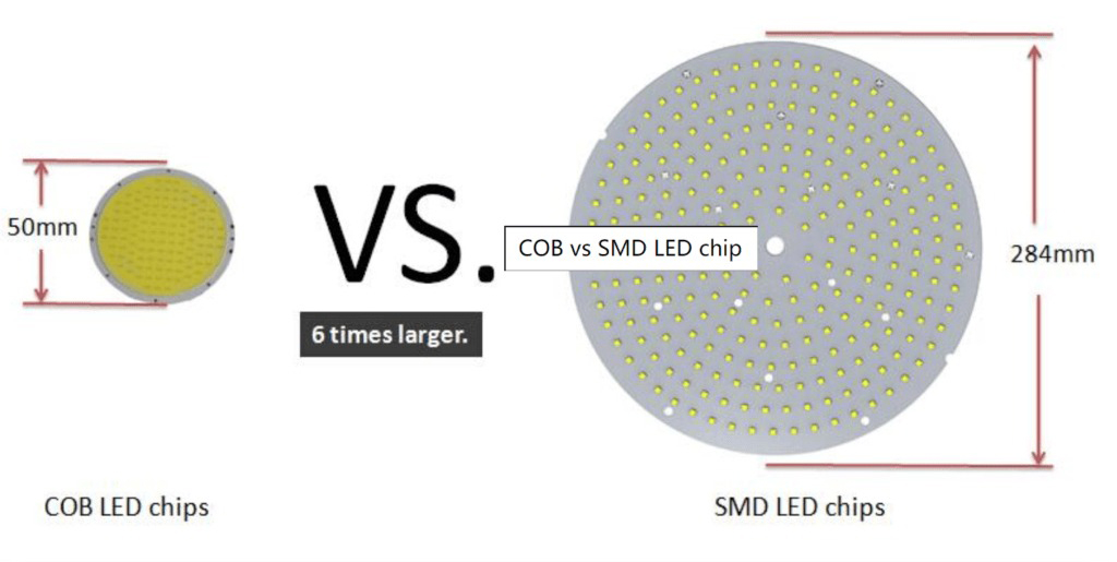
COB displays, with their surface light source characteristics, provide viewers with finer and more uniform visual experiences. Compared to the point light source of SMD, COB offers more vivid colors and better detail handling, making it more suitable for long-term, close-up viewing.
3.2 Comparison of Stability and Maintainability
While SMD displays are easy to repair on-site, they have weaker overall protection and are more susceptible to environmental factors. In contrast, COB displays, due to their overall packaging design, have higher protection levels, with better waterproof and dustproof performance. However, it should be noted that COB displays usually need to be returned to the factory for repairs in case of failure.
3.3 Power Consumption and Energy Efficiency
With an unobstructed flip-chip process, COB has higher light source efficiency, resulting in lower power consumption for the same brightness, saving users on electricity costs.
3.4 Cost and Development
SMD packaging technology is widely used due to its high maturity and low production cost. Although COB technology theoretically has lower costs, its complex manufacturing process and low yield rate currently result in relatively higher actual costs. However, as technology advances and production capacity expands, the cost of COB is expected to further decrease.
4. Future Development Trends
RTLED is a pioneer in COB LED display technology. Our COB LED displays are widely used in all kinds of commercial LED displays due to their excellent display effect and reliable performance. RTLED is committed to providing high-quality, one-stop display solutions to meet our customers’ needs for high-definition displays and energy-saving and environmental protection. We continue to optimize our COB packaging technology to bring our customers more competitive products by improving light source efficiency and reducing production costs. Our COB LED screen not only have excellent visual effect and high stability, but also can operate stably in various complex environments, providing users with a long-lasting experience.
In the commercial LED display market, both COB and SMD have their own advantages. With the increasing demand for high-definition displays, Micro LED display products with higher pixel density are gradually gaining market favor. COB technology, with its highly integrated packaging characteristics, has become a key technology for achieving high pixel density in Micro LEDs. At the same time, as the pixel pitch of LED screens continues to decrease, the cost advantage of COB technology is becoming more apparent.
5. Summary
With continuous technological advancements and market maturation, COB and SMD packaging technologies will continue to play significant roles in the commercial display industry. We have reason to believe that in the near future, these two technologies will jointly propel the industry towards higher definition, smarter, and more environmentally friendly directions.
If you are interested in LED displays, contact us today for more LED screen solutions.
Post time: Jul-17-2024